
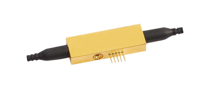
Overview
Thin‑film lithium niobate (TFLN) is a wafer structure formed by thinning bulk lithium niobate crystals to the nanometer scale through advanced processes and bonding them onto an insulating substrate. TFLN technology overcomes the limitations of bulk lithium niobate—large form factor, difficulty in integration, and high driving voltage—while fully preserving its excellent electro‑optic properties. Its exceptionally strong linear electro‑optic effect enables device bandwidths exceeding 110 GHz, supporting next generation ultra high speed optical modules such as 1.6T and 3.2T. Driving voltage can be controlled within 1.8V, directly compatible with low voltage CMOS driver chips. With high refractive index contrast and strong optical field confinement, device surface area can be reduced by approximately 100 times, significantly improving device footprint. Leveraging its outstanding electro‑optic, acousto‑optic, and nonlinear optical properties. TFLN is widely used in ultra high speed optical communications, optical computing, quantum communications, and LiDAR, among other advanced applications.
Applications
- Fiber optic RF
- Microwave photonic radar
- Optical pulse generation
Product Features
- TFLN
- Low half‑wave voltage
- Integrated photodiode
- Long‑term stability and reliability
- Single‑drive, zero‑chirp operation
Please log in to view the full article.
